My previous project to create breakout boards for ESP-12E and ESP-12F modules was mainly to enable rapid prototyping for this project. The goal for this project was to create an Arduino-compatible dev board that had some nice quality-of-life features.
Creating your own dev board for an IC or module is a great way to learn new skills and hopefully end up with a useful product at the end.
This blog is a writeup of the obstacles along the way, and what I ended up with in the end, and things I would change for future revisions.
Background #
Previously, I’d been cobbling together some sensors for houseplants that record the soil moisture level and report it over MQTT for use inside Home Assistant. The sensors were usually a combination of an ESP-12F (mounted on a breakout board), resistors, capacitors, and the moisture sensor itself all plugged into a mini breadboard.
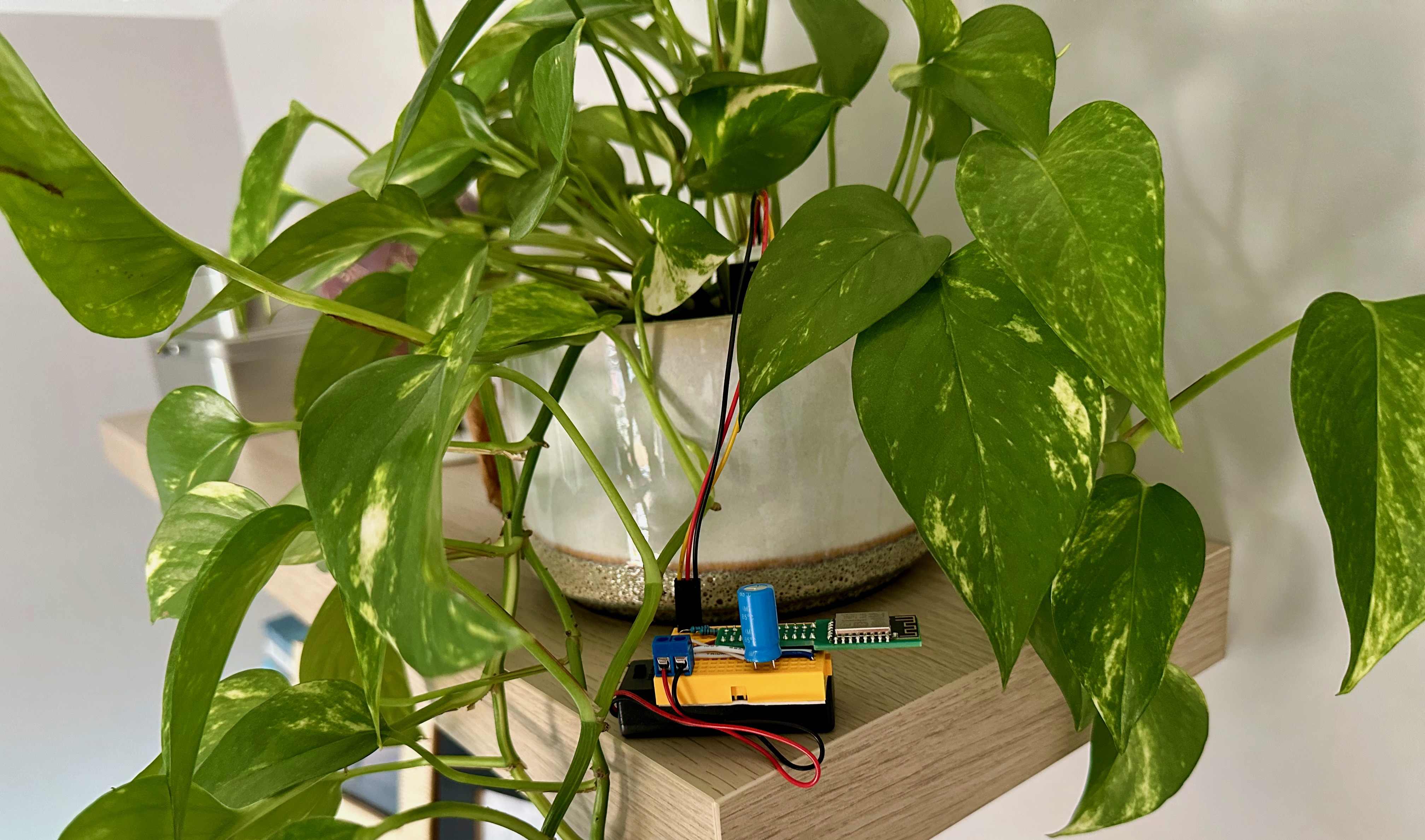
These sensors spend 99% of their time in Deep Sleep mode and wake up roughly every hour to record the latest reading and then go back to sleep.
When the ESP-12F is in “Deep Sleep” it draws around 15µA so it can last on batteries for a long time (~1 year).
This all works fine, but the non permanent and fragile/flakey construction of breadboard-based sensors wasn’t particularly robust and was, in a word, janky. Instead of mini breadboards or stripboard circuits, I decided to take the plunge and design my own PCBs for these sensors.
Wishlist #
My original wishlist for a specialized board for sensors looked like this:
- Low power (no additional drain when using
ESP.deepSleep()) - USB-C to Serial connection for programming, no drivers required
- Onboard ~5V to ~3.3V LDO voltage regulator
- Voltage divider for the lone analog input pin
- (The ESP-12 boards can only tolerate 0-1V on their analog pin)
- All the appropriate strapping pins to enable normal booting
- Reset button
- Battery charging / protection IC
- Breadboard friendly
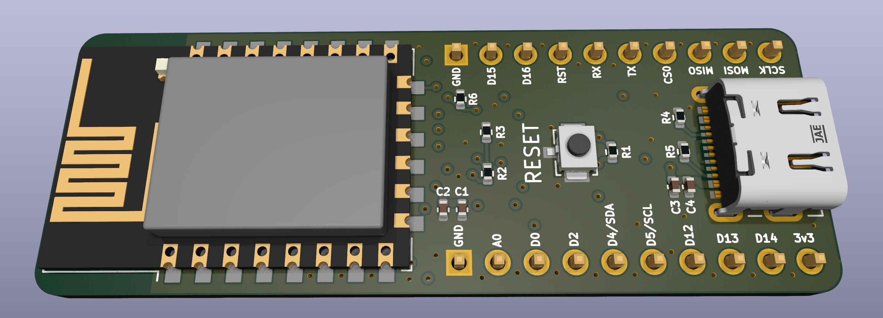
Design #
Not going to lie, this was quite a struggle since I was pretty new with KiCAD and designing anything more complicated than the breakout board was pretty challenging.
Ultimately I ended up nixing the battery charging and just focused on making a dev board that could be quite versatile, and useable for many different types of projects, rather than solely low-powered sensors.
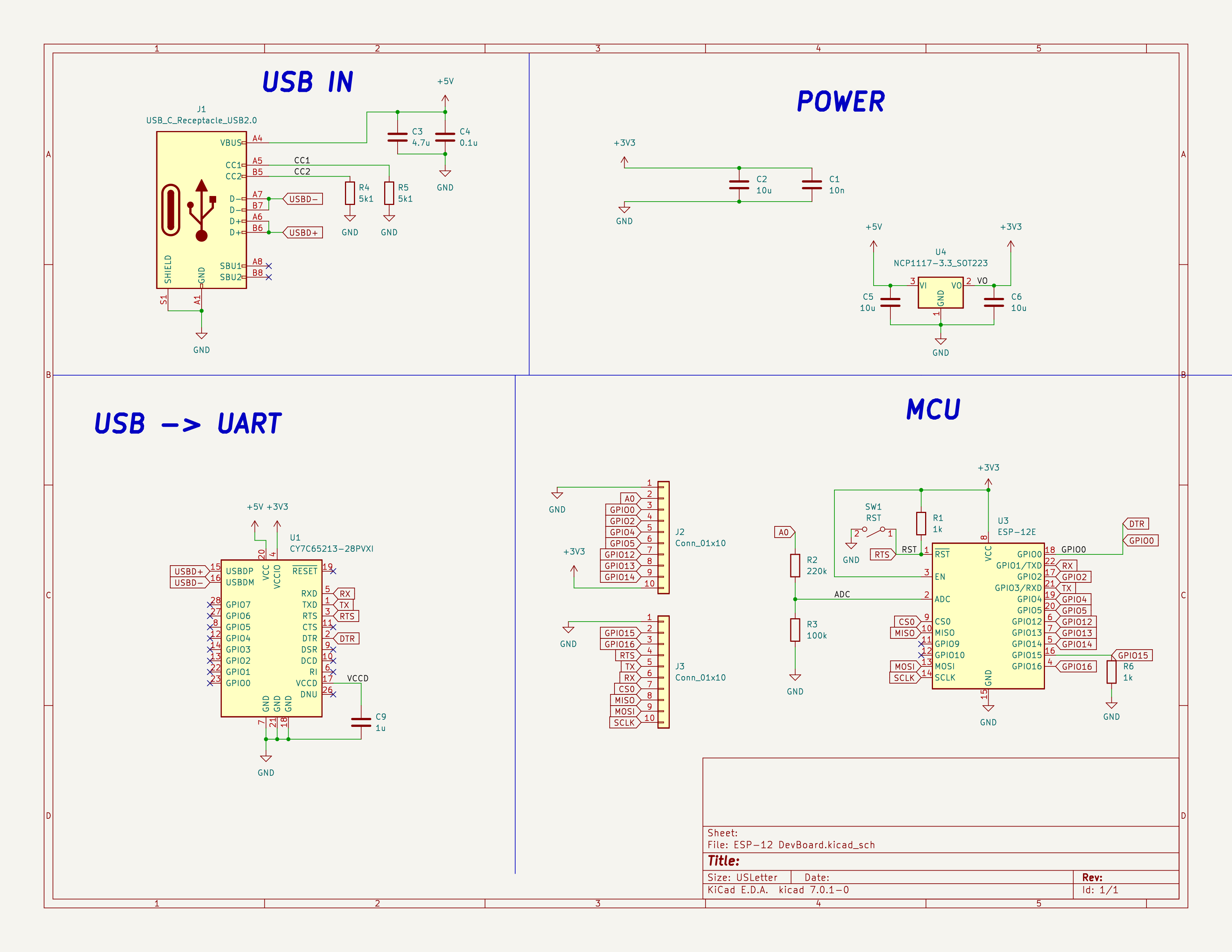
Some notes here
- 220k and 100k resistors used to divide ~3.3v down to ~1v for the analog pin
- Various decoupling capacitors were mainly derived from component datasheets
- 5.1k resistors on the
CCpins of the USB-C connector to tell the host to send 5V (required for USB-C to USB-C cables to work properly) - Breakouts for almost every pin (GPIO9/10 are not useable anyway)
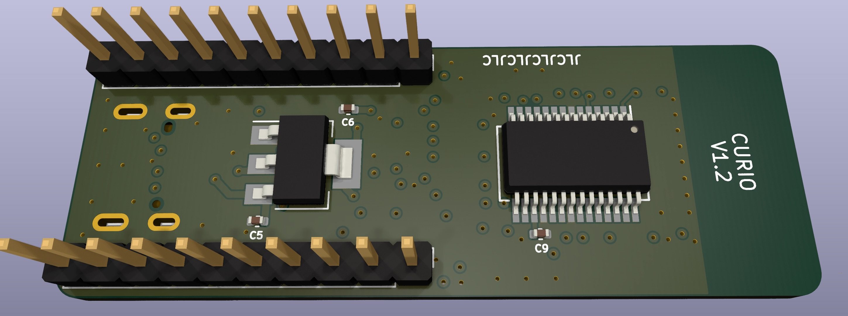
USB to Serial IC #
Originally I had looked at the USB to Serial boards I had laying around and
saw that the FTDI FT232RL was used on almost all of them, so why not me?
At the time of building out this dev board however they were out of stock
everywhere. I did however discover another IC that claimed to be
pin-compatible with the FT232RL: the CY7C65213 from Cypress Semi (a.k.a.
Infineon). I used the CY7C65213-28PVXI specifically and I can confirm that it
works just as well as the FTDI chips!
LDO #
ESP boards generally run on 3.3V but USB provides around 5V. To step VBUS down
to 3.3V I chose the NCP1117-3.3 which comes in a neat little SOT223
package.
This is where the pin difference between the Cypress and FTDI chips comes to light. The original FTDI chip actually has an internal regulator that ouputs 3.3v so technically I could have managed without a dedicated LDO at all.
That said, I’m not sure what kinds of current the FTDI’s regulator can deal
with. The ESP8266 can spike up to 600mA for a millisecond or two when
connecting to WiFi (I’m going to do another blog specifically about that later!)
and the FT232RL datasheet seems to imply that its 3v3 pin maxes out at 50mA.
So either way, the dedicated LDO regulator seems like a good idea.
Prototyping #
Once all the parts were acquired, it was time to prototype the board. This approach helps to find design flaws before committing to a full PCB.
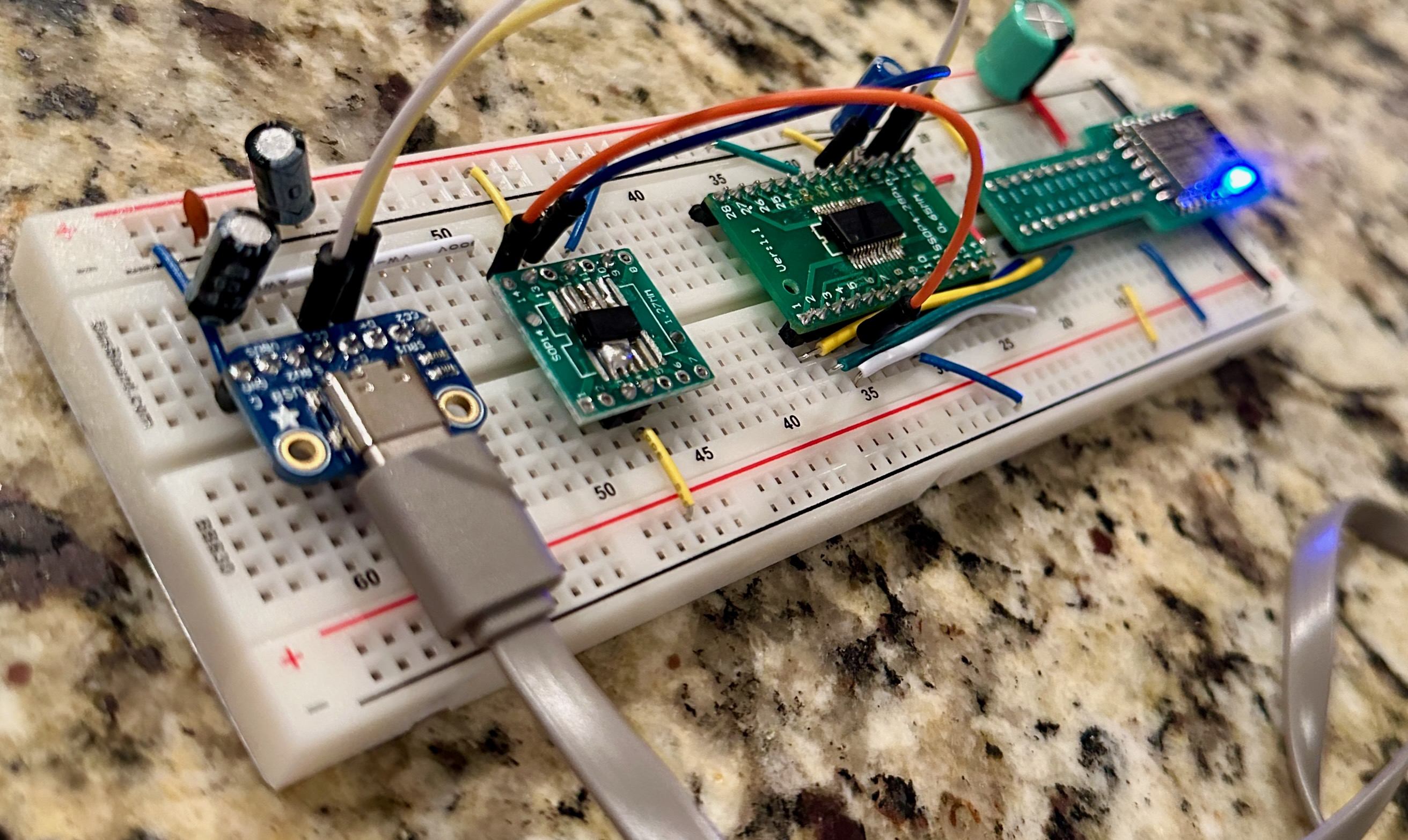
It worked! In the above photo you can see the USB-C connector, the LDO, the USB -> Serial IC and the ESP-12F module at the very end. The LDO and Cypress chips are mounted onto these little SMD breakout boards I found on Amazon. Super useful for prototyping.
After a bunch of testing, everything appeared to work as intended!
PCB Design #
This was the step that took the longest out of this whole process by far.
Initially the board was going to be just 2 layers (top/bottom) with signals on both sides. Very quickly it became apparent that wasn’t going to work given the space constraints. I added 2 more layers to allow for more routing options which helped a LOT.
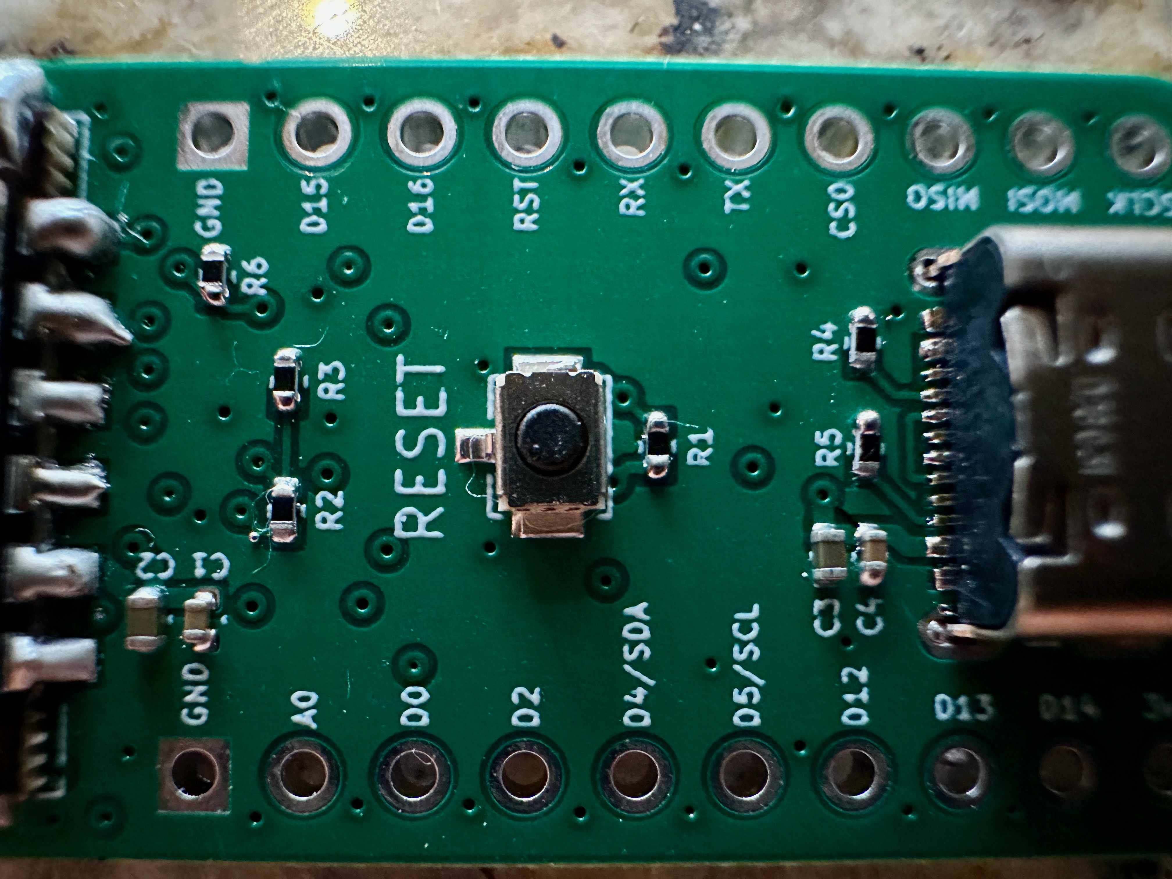
In terms of physical sizing, for the board to be breadboard friendly, it needed space for pin headers which had to be some multiple of 2.54mm apart. Additionally it would be good if that distance was as small as possible to maximize access to breadboard holes on either side.
I landed on 15.24mm between pin headers, which equates to exactly 6 breadboard holes. Some ESP-12 carrier boards and breakouts I found online actually require 2 breadboards to accomodate their width, so I definitely wanted to avoid that.
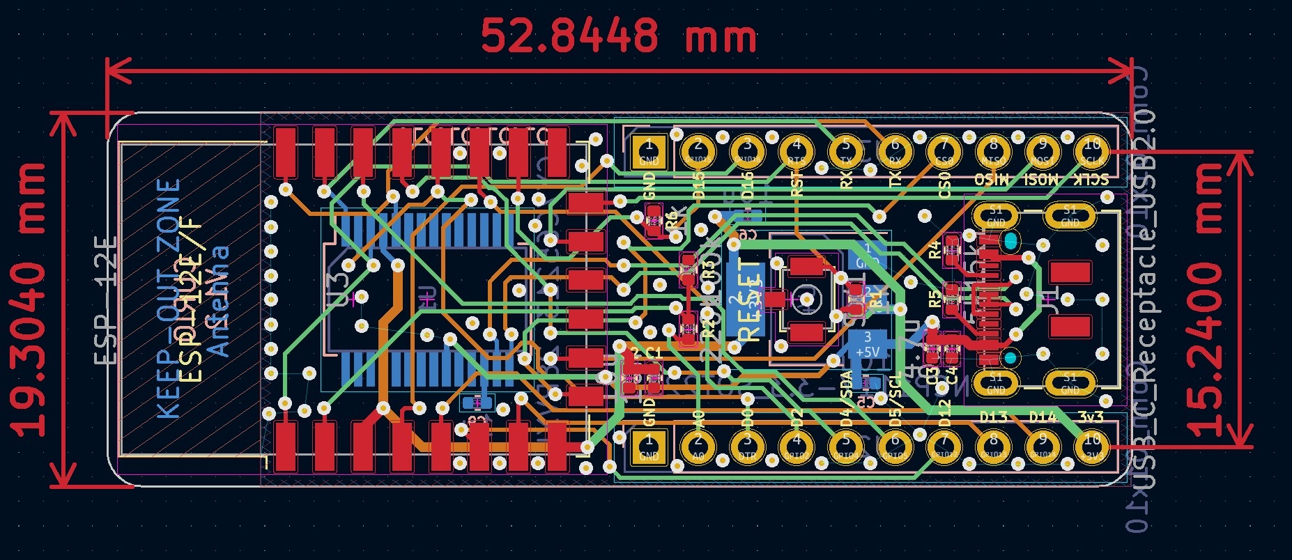
Not particularly great from an aesthetics perspective, but it’s definitely functional and generally(?) symmetrical.
Fabrication #
I ended up exporting the Gerber files and sending them to JLCPCB for production.
A few days later, these appeared in the mail!
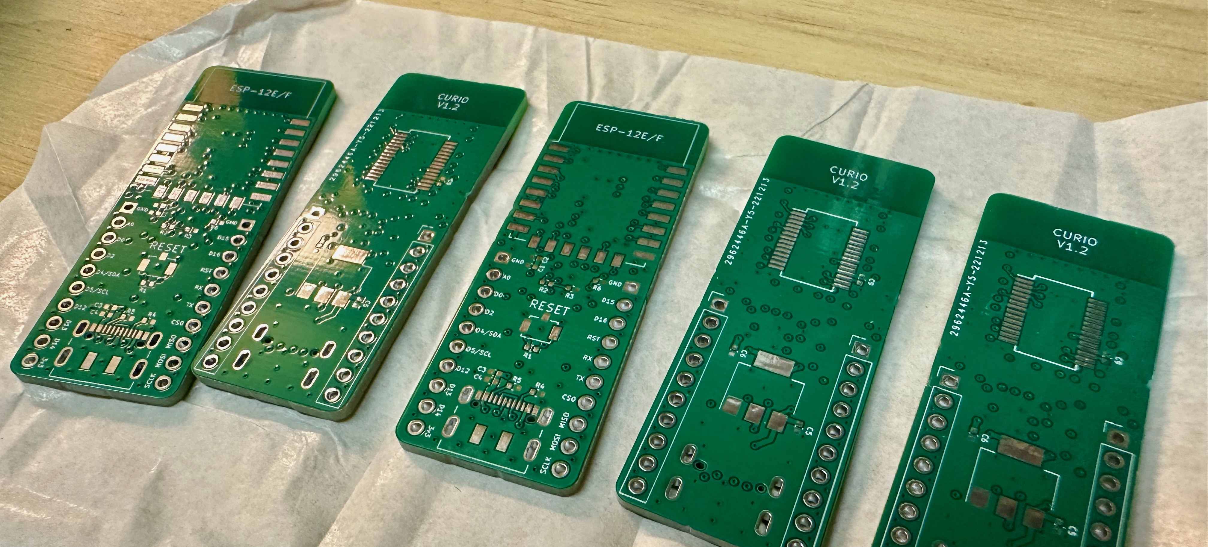
Some things I noticed right away
- The quality from JLCPCB is really good, especially since these were just $2!
- The silkscreen size I chose is SO SMALL it’s just barely legible
- 0402 components that I chose might have been a mistake…
- I accidentally did NOT choose the lead-free finish. Make sure to wash your hands thoroughly after handling these boards!
Assembly #
Assembling the boards was yet another challenge. I had never done hot air soldering OR SMD soldering before other than a tiny bit of practice to mount components onto SMD breakout boards. Also, there were only 5 of the CURIOs made at JLCPCB so I didn’t want to mess up too badly. I figured if I just take my time and be methodical about it, it should be OK. That was until I saw the size of all the passive components I had ordered…
0402 components are almost comically small. It’s like handling a single grain of sand. So not only am I hot air and SMD soldering for the first time, but also managed to choose one of the most challenging sizes!
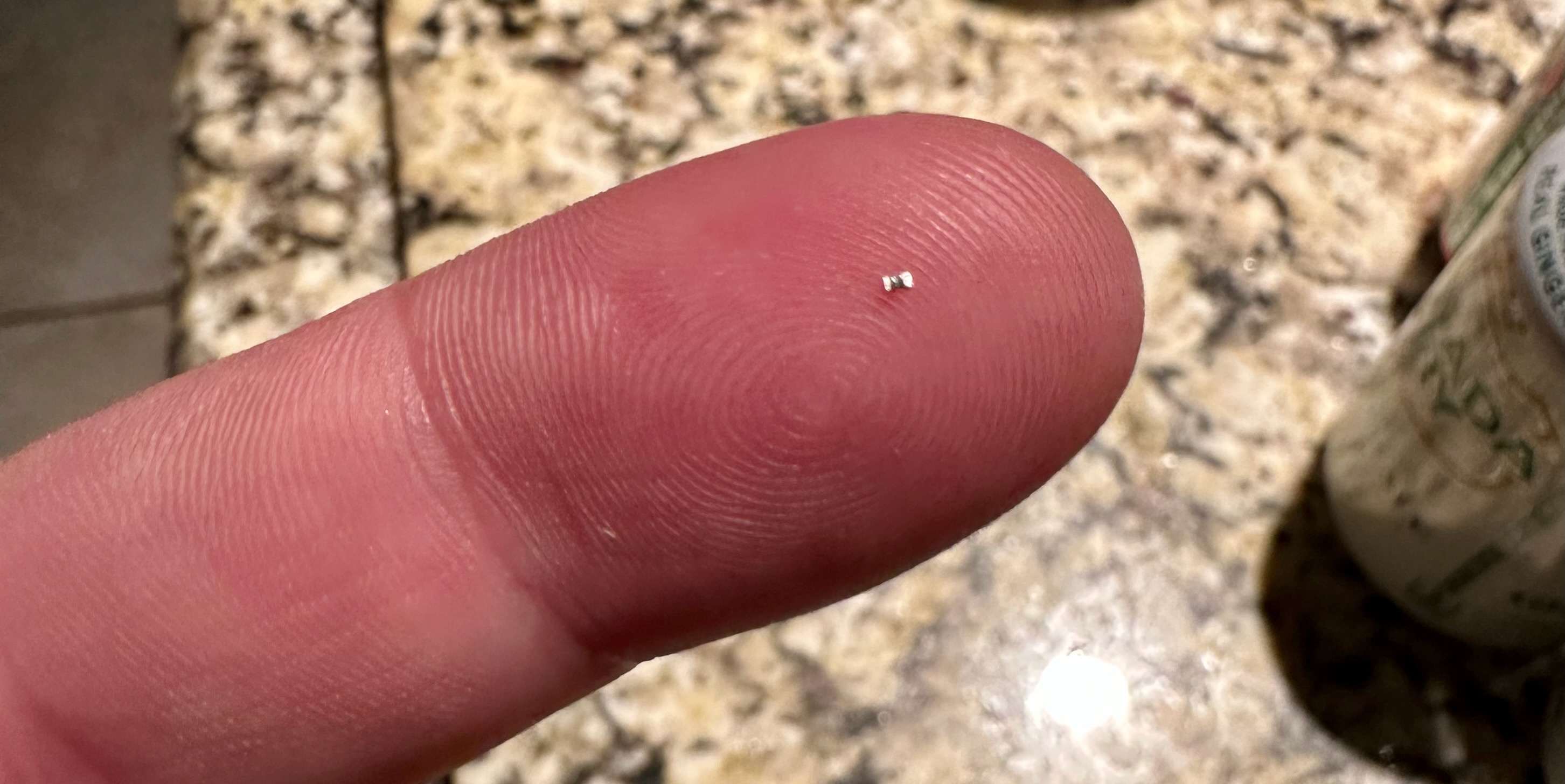
You can get also components that are 01005 sized. They just look like dust!
A couple of things I learned while assembling these boards using hot air soldering:
- Components can get blown away easily, use low airflow settings
- Be wary of tombstoning. Make sure all the pads of each part are getting heated at the same time and rate
- Be patient. It can a minute or two to fully reflow the solder and position the part
- Use good tweezers to handle the components. I have fine (i.e. small) tweezers but they are quite cheap and not the best quality.
- Be patient…
I assembled in stages. Starting with the smallest components first and in logical groupings by their location. That way you can reflow several things at once.
In the end, I ruined one of the boards with some overenthusiastic appliction of my soldering iron, but I ended up assembling two of them successfully ✅.
Testing #
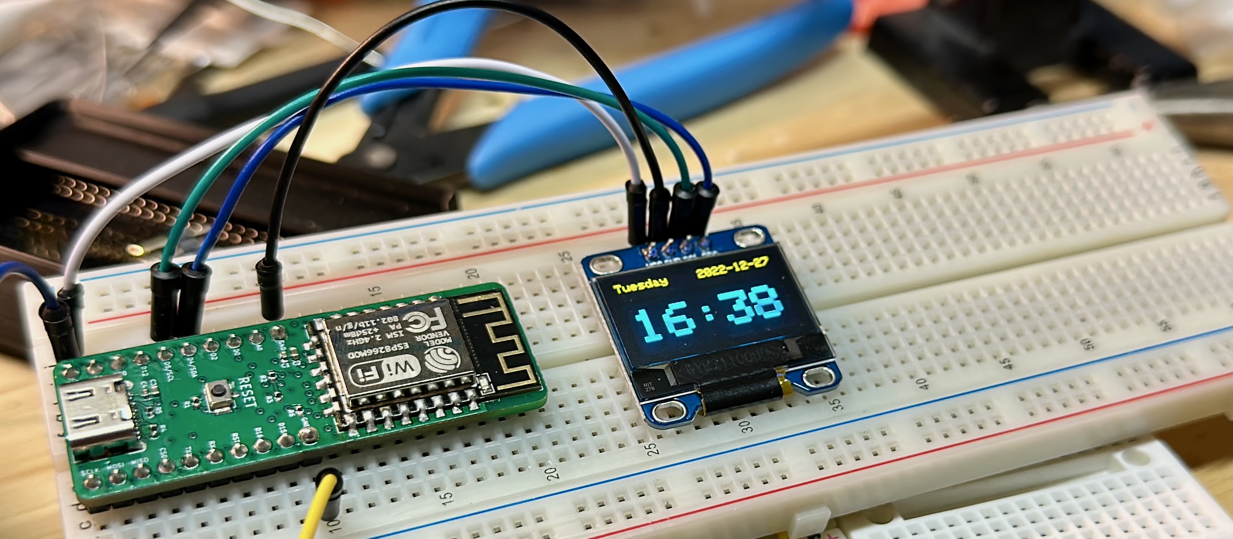
Plugging the device into my laptop via USB-C I was able to see it as a serial
device 🎉. In addition I was able to get it to blink its LED by uploading a
Blink sketch to it from the Arduino IDE. I chose Generic ESP8266 Module as
the board, and then everything else worked as expected!
A problem arose while testing the deep sleep capabilities however.
While the module is deep sleeping, the USB to Serial chip is still awake and having a great time sitting there idle and drawing current 😭.
Therefore, without some sort of revision this dev board is NOT particularly well-suited to running on batteries for an extended period of time. Bummer.
It’s not crazy but it wouldn’t have a particularly good battery life.
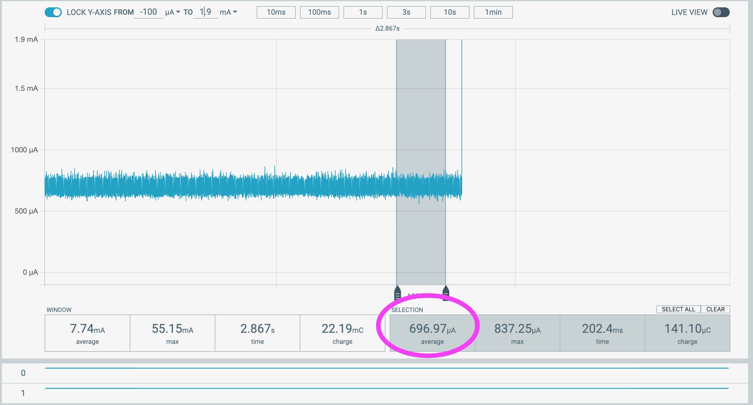
700µA isn’t exactly a huge amount but it is 46.6 times more current draw than I expected. And likewise the battery life with the CURIO would be 46 times less than one of my janky breadboard sensors that just uses the bare module.
So how would I fix this? Well, when running on batteries, the power is applied
to the 3v3 breakout pin. When connected via USB the power takes a different
path.
So theoretically there is probably some way to isolate the LDO + Serial IC from the ESP module with one or more diodes, such that when 3.3V is applied at the pin, the power ONLY goes to the module, and does not leak into the LDO or the Serial chip.
Any other suggestions? Leave a comment!
Reflection #
While the final product was unfortunately not really fit for its original intended purpose, I have been able to put a few of them to work as IoT-button type devices. They are always plugged in and so I don’t have to worry about battery life. Also just as a general dev board they are really great, and have a ton of functionality.
Overall, the project taught me a huge amount about a wide variety of topics like
- PCB design best practices like component placement, noise, voltage references
- SMD soldering with hot air
- Choosing/sourcing parts
Mistakes / Opportunities #
I already mentioned the power consumption being too high as a big flaw, but
there are quite a few other things I would change in a v2.0 revision of the
CURIO to make it even better
No BOOT button #
I thought I was being clever by leaving this out. You’re programming it via USB!
DTR on the serial IC is asserting GPIO0 automatically! What do you need a
button for!?
Well 🤦♂️ it turns out it’s quite easy to write code that causes the module to just boot loop, or do something which otherwise blocks uploading new code. In those cases you have to put the bootloader into download mode.
The workaround in practice for the CURIO is to just use a jumper wire to short
GPIO0 to GND and then press the RESET button. So it’s not too much work
to get around this particular design flaw. A button would be better / more
convenient however.
Bad stackup #
This was something I didn’t really think too much about until a friend of mine who does this for a living educated me.
The 4 layer stackup I used was GND-Signal-Signal-GND. Unfortunately what this means is that if a signal jumps from the one internal layer to the other, through a via for example, its reference to ground is also flipping from the top plane to the bottom plane.
This switching can introduce noise/interference/ringing and wreak havoc on any high speed circuitry. Luckily for me, the most sensitive thing I routed was the USB D+/D- traces, which are actually just USB 2.0 for this project. The real sensitive stuff (wifi) is self-contained within the ESP module under the RF shield. If I was doing USB High-Speed or power filtering stuff it would have been a dealbreaker for the project.
In practice for this board, it doesn’t really make much of a difference. Maybe the WiFi isn’t as strong/capable as it would be otherwise, but I’m not 100% sure.
For future similar designs I would stick to a Signal-GND-GND-Signal stackup, to keep the ground references close and the noise low.
0402 was too small #
Pretty self-explanatory, but I should probably have gone up a few sizes. Maybe 0805 for example. 0402 is nice for keeping things small, but a bit of a pain to assemble.
Unfortunately, I am now the proud owner of hundreds of leftover 0402 passive components, so I will probably still put those to use in future projects 🙈.
Fabrication Options #
Next time I will definitely opt for the HASL lead-free finish, if not the ENIG gold plated finish. I think keeping exposure to harmful elements to a minimum is probably a reasonable thing to do!
Silkscreen was another fabrication option (but set at PCB design time) that I would probably tweak/improve in a future revision. To make it larger, and maybe more creative!
Get the repo #
I hope this was somewhat helpful to anyone reading. As usual leave comments and questions below.
If you want to get the KiCAD project yourself, you can get it from https://github.com/phybros/curio
Comments